nanoCentre Belgrade spacer
Imaging    Characterisation    NanoFab    Modeling    Life Science    Booking  
nano Centar Beograd spacer
HOME                    About                   Scientific Advisory Board                   Organisation                   Equipment                   Contact  
nano Centar Beograd spacer


Center for Characterisation


Fast Screening


SPM


Optical Characterization


Transport and Magnetic Measurements


Structural Characterization


The Center for Characterization provides instruments for general materials' characterization regardless of the sample size. Such characterization section deals more with the materials general properties rather than its appearance.

The instrumentation is grouped in four sections:
  • Fast Screening
    (ICP-MS, TGA/DTA/DSC, Routine AFM, XFS, UV-VIS, FTIR, Dynamic Light Scattering, Polarizing Optical Microscope)
     
  • SPM
    (AFM High Resolution, AFM/Confocal Raman, AFM SNOM)
     
  • Optical Characterization
    (Fluorometer with lifetime module, FTIR/FT Raman, UV-VIS, NIR Spectrometer, Photonic Laboratory: various laser sources with OPO,optical cryostat, photo-luminescence, resonance enhanced Raman, SERS, PLQE and ELQE, radiative life-time, photo-conductivity, SHG/THG/SFG, photovoltaic response)
     
  • Transport and Magnetic Measurements
    (Pulse-EPR, SQID, Cryogen Four Probe)
     
  • Structural Characterization
    (XRD (SAXS, IP-GID), XPS/UPS)
     

Fast Screening

Fast Screening section is meant for the first time users of the Facility that are not certain about basic properties of their newly synthesized materials. There, with some routine measurements, they are able to get information about the sample composition (ICP-MS, XFS), its thermal stability (TGA/DSC), basic optical properties (UV-VIS, FTIR), particle size and surface morphology (light scattering, AFM,) and so on. The purpose of this section also is to prevent accidental contamination of more specialized and expensive equipment that should not be used without prior knowledge of the sample basic properties.


SPM

SPM unit provides various devices for surface imaging and characterization based on scanning probe microscopy. The unit is equipped with High Resolution AFM, ambient, low pressure and low temperature AFM. Also, the unit provides SNOM and AFM imaging in liquid for biological samples. In addition, the Center is equipped with Confocal Raman integrated within AFM and optical profilometer.


Optical Characterization

Optical Characterization section is divided in two parts:

  • Standard Optical Characterization and
  • Photonic Laboratory.

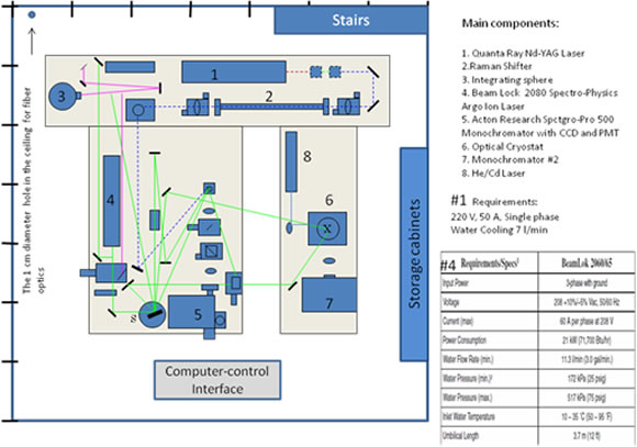
The former is featuring the state of the art commercial instruments for absorption, emission and inelastic light scattering measurements that can be performed in a broad spectral range with superb sensitivity, resolution and accuracy (see the capital equipment selection list). Photonic Laboratory is dedicated to users requiring more advanced optical measurements for which no commercial instruments are available. It features several different laser sources, spectrometers, and sensitive light detectors in the UV, VIS and NIR region, all assembled on a couple of large optical tables. The flexible optical setup allows for number of different measurements to be performed sequentially by using a simple set of optical switches. In this way the laser output is sent through various sets of optical components required for one type of measurements, which are attached permanently on the optical table. These include photo-luminescence (PL), resonance enhanced Raman (RAR) , surface enhanced Raman (SERS), photo- and electro-luminescence quantum efficiency (PLQE and ELQE), radiative life-time, photo-conductivity, nonlinear optical response (SHG,THG, SFG), photovoltaic response, and others. A state of the art optical cryostat permits these measurements to be performed as a function of temperature, simultaneously with electric transport measurements when needed.

The output of various laser sources is coupled by a fiber-optical network to remote instruments in other laboratories. In this way photo-induced magnetic response or photo-conductivity measurements of thin films, nano-tubes or even small organic molecules is possible by introducing a desired laser output into the optical cavity of EPR or magnetic four probe cryogenic station for instance (see below). Particular attention is given to the choice of laser sources where both simplicity of operation and advanced performance is required simultaneously. This is possible to achieve thanks to the most recent technological advances in the field of laser spectroscopy. A good example is the Coherent compact optical parametric oscillator (Chameleon), a tunable Ti:Saphire laser accessing an unprecedented automated tuning range of 340 nm to 4000 nm with simple touch screen controls and no manual intervention. The unique capabilities of the Photonic Laboratories distinguish NanoCenter Serbia from other institutions of the kind and is expected to fulfill the needs of a wide range of researchers from different fields and institutions in the country and abroad. It also supplements the existing optical facilities in the Institute of Physics and others that more specialized for certain type of spectroscopy measurements.


Photonic laboratory scheme (located in basement):


Transport and Magnetic properties

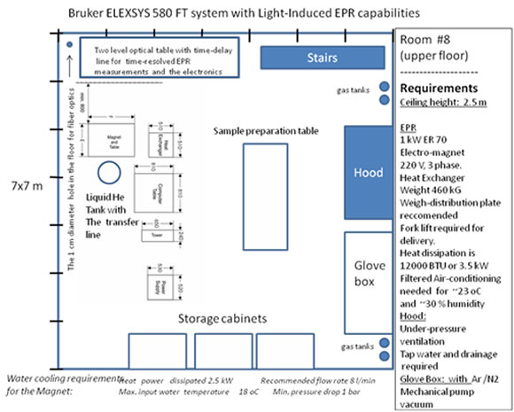
Transport and Magnetic properties of nano-materials are of particular interest for novel technological applications. This section of the User Facility features several state of the art instrumentation from leading manufacturers. The Bruker ELEXSYS E 580 X-band EPR spectrometer allows for both continues wave and pulsed operations and permits detection of paramagnetic species induced by light. There has been an increasing awareness among pharmaceutical industry that the exposure of certain medicaments to sunlight can induce free radical formation and thus alter the drug. A detailed understanding of light-induced charge-transfer phenomena is of fundamental importance for light detectors, photo-voltaics and photo-synthesis as well. As already mentioned, we couple photonic laboratory with the Laboratory for Magnetic and Transport measurements, which will allow detailed investigations of such phenomena.

The MPMS VSM Magnetometer from Quantum Design offers ≤ 10-8 emu sensitivity with only few seconds of data averaging. By combining the speed of a vibrating sample magnetometer with the sensitivity of a SQUID (Superconducting Quantum Interference Device), this system offers major advances in data acquisition and is perfectly suited for User Facility where efficiency is one of the key requirements. The SQUID VSM comes with a 4He-based Pulse Tube cooler which eliminates the need for liquid cryogens, yet another advantage over the SQUID magnetometer. It should be mentioned that classical SQUID does have some capabilities that are absent in vibrating sample magnetometer. For instance, it allows for simultaneous magnetic and transport measurements and/or it can reveal magnetization anisotropy. There is an operational SQUID magnetometer in the Vinca Institute and is formally opened to outside users. It would be therefore vise to augment this particular instrument to the User Facility in case that some measurements cannot be performed by MPMS VSM Magnetometer in the Nano-Centre.

The new Lake Shore CCR-EMPX-HF micro-manipulated probe station is perfectly suited for the measurement of magneto-transport, electrical and electro-optical (i.e. the photoconductivity), parametric, high Z, DC, RF, and microwave properties of materials and test devices. Nanoscale electronics, quantum wires and dots, semiconductors, superconductors, and spintronic devices are typical materials measured in a CPX-VF. A wide selection of probes, cables, sample holder options are offered. As with the EPR instrument, the fiber-optics network couples laser sources from Photonic Laboratory to allow light assisted transport measurements to be performed.

The laboratory for Transport and Magnetic properties (located above Photonics laboratory)


Structural Characterization

Structural Characterization of solid state samples often requires a combination of analytical techniques. Some of these techniques are elemental analysis, mass spectrometry, NMR spectroscopy, and X-ray diffraction. There are a large number of different types of instruments for each of these methods and techniques available on the market. Some of those are scattered among several scientific institutions in Belgrade and are in principle accessible to a broader scientific community. There are two groups specialized in mass spectrometry, one in Vinca and one at the Technology University of Belgrade. There is a liquid NMR spectrometer in the Department of Chemistry in Belgrade, which is well utilized and is serving users from other institutions on a regular basis. There are also a few operational X-Ray diffraction instruments.

When considering equipment for this section of the NanoCentre, attention was paid not to duplicate some of the existing advanced instruments for characterization, such as mass spectrometry for instance. At the same time there is an apparent lack of some instruments that are particularly suited for nano-science, which are normally present in the centers of that kind worldwide. Taking all of this into account, the following instrumentation has been proposed in this section.

An XPS/UPS spectrophotometer capable of measuring the elemental composition, empirical formula, chemical state and electronic state of the elements that exist within a material. The particular Nano-ESCA from Omicron offers chemical state mapping with unsurpassed lateral resolution (<500 nm achieved under laboratory conditions). The instrument allows analyzing smallest sample structures giving chemical state information beyond the limits of other high lateral resolution techniques such as scanning Auger and TOF SIMS. In addition, the instrument provides quantitative information on the very local work function and local sample charging. The spectroscopy capabilities of the NanoESCA can be completed by the µARUPS option which allows analyzing the k-space from µm-areas e.g. small grains in a polycrystalline surface with ultimate angular acceptance. The system offered by Omicron contains an UHV analysis chamber with 3 ports for the optional excitation sources: UV light (mercury or deuterium source); VUV light (He discharge source HIS 13 with fine focus upgrade); laboratory X-ray source.

The Nano ESCA imaging XPS/UPS analyzer consists of an imaging lens system with a double hemispherical electron analyzer. Images are detected by means of two detectors with channel-plates and a fluorescent screen. One detector is for the XPS imaging (energy filtering) and the other displays high intensity images – PEEM (without energy filtering). Images are acquired by one Peltier cooled slow scan CCD camera alternatively at the XPS and PEEM imaging detector. The momentum microscope extension is an additional set of lenses allowing the observation of the momentum distribution of photo-excited electron states in an energy plane through the Brillouin zone by an energy sequence of parallel cuts through the zone. The integrated k-space lens and dedicated electron optics allows for fast switching from real space imaging to reciprocal space imaging from a well defined sample area. Equipped with the transfer lens, the momentum microscope is suitable for k-space and Fermi surface mapping.


The X-Ray diffraction instrument, D8 DISCOVER with DAVINCI design, increases ease-of-use with real-time component detection, plug-and-play functionality and fully integrated 2-dimensional XRD capabilities. These unique features allow the user to easily switch between all materials research X-ray diffraction applications, including reflectometry, high-resolution diffraction, grazing incidence diffraction (IP-GID), small angle X-ray scattering (SAXS), as well as residual stress and texture investigations. In particular, for micro-diffraction and ultra-fast reciprocal space mapping, the new two-dimensional VǺNTEC-500 detector with 2048x2048 channels at 144 cm2 active area provides highest sensitivity for detecting even the weakest diffraction signals in short measurement times. The D8 DISCOVER with DAVINCI design is designed to meet all the latest X-ray safety regulatory requirements, providing scientists peace-of-mind. An integral part of the D8 DISCOVER with DAVINCI design is the new software with consistently implemented automation functionality. An X-ray optics module, a detector, or any accessory mounted onto the instrument registers itself in real-time with its relevant parameters and analytical capabilities, including powerful detection of possible component conflicts. The factory-aligned, snap-lock X-ray optics provide true ‘plug-and-play’ functionality, including automatic and tool-free switching of the diffraction geometry with minimal user intervention. The DIFFRAC.SUITE offers intuitive operation based on a graphical user interface that can be customized to match the operator’s requirements.